Key Highlights from Jensen Huang’s Keynote 2024 GTC
- Introduction of Blackwell Architecture: A leap forward in AI technology, promising to revolutionize various industries.
- Project GROOT Announcement: Showcases advancements towards the human-robot future, bringing us closer to more interactive and capable robots.
- Collaboration with Apple Vision Pro: Nvidia’s venture into the Omniverse, aiming to enhance virtual reality experiences.
- Digital Twin of the Planet: An ambitious project to recreate the entire planet digitally for better weather forecasting and more.
Notable Announcements and Developments
- Humanoid Robots in Development: Demonstrated potential applications across factories, healthcare, and science, signaling the future may not be far off.
- Isaac Perceptor SDK: New software aimed at robotic arms and vehicles, providing them with greater insight and intelligence.
- Omniverse Cloud Streaming to Apple Vision Pro: A step towards more immersive virtual environments, powered by Nvidia’s cutting-edge technology.
- Partnership with Nissan: Highlighted the potential for AI in customizing new car options, showcasing a blend of technology and consumer choice.
- Siemens Collaboration: Nvidia’s technology will be used to boost productivity and efficiency in virtual warehouses, marking significant industrial application.
- Advancements in Healthcare: Nvidia building models to aid researchers worldwide, speeding up drug discovery processes.
- Earth-2 APIs for Better Weather Forecasting: A collaboration with The Weather Company to improve predictions and save lives.
NVIDIA Blackwell GPU Architecture Overview
Introduction
The NVIDIA Blackwell architecture introduces a significant leap forward in generative AI accelerator technology, incorporating the B200 and B100 accelerators. Named in honor of Dr. David Harold Blackwell, a pioneer in statistics and mathematics, this next-generation architecture is designed to redefine performance, flexibility, and efficiency in the realms of datacenter and high-performance computing (HPC).
Nvidia Blackwell Chips
| Specification | GB200 | B200 | B100 | HGX B200 | HGX B100 |
|---|---|---|---|---|---|
| Configuration | 2x B200 GPU, 1x Grace CPU | Blackwell GPU | Blackwell GPU | 8x B200 GPU | 8x B100 GPU |
| FP4 Tensor Dense/Sparse | 20/40 petaflops | 9/18 petaflops | 7/14 petaflops | 72/144 petaflops | 56/112 petaflops |
| FP6/FP8 Tensor Dense/Sparse | 10/20 petaflops | 4.5/9 petaflops | 3.5/7 petaflops | 36/72 petaflops | 28/56 petaflops |
| INT8 Tensor Dense/Sparse | 10/20 petaops | 4.5/9 petaops | 3.5/7 petaops | 36/72 petaops | 28/56 petaops |
| FP16/BF16 Tensor Dense/Sparse | 5/10 petaflops | 2.25/4.5 petaflops | 1.8/3.5 petaflops | 18/36 petaflops | 14/28 petaflops |
| TF32 Tensor Dense/Sparse | 2.5/5 petaflops | 1.12/2.25 petaflops | 0.9/1.8 petaflops | 9/18 petaflops | 7/14 petaflops |
| FP64 Tensor Dense | 90 teraflops | 40 teraflops | 30 teraflops | 320 teraflops | 240 teraflops |
| Memory | 384GB (2x8x24GB) | 192GB (8x24GB) | 192GB (8x24GB) | 1536GB (8x8x24GB) | 1536GB (8x8x24GB) |
| Bandwidth | 16 TB/s | 8 TB/s | 8 TB/s | 64 TB/s | 64 TB/s |
| NVLink Bandwidth | 2x 1.8 TB/s | 1.8 TB/s | 1.8 TB/s | 14.4 TB/s | 14.4 TB/s |
| Power | Up to 2700W | 1000W | 700W | 8000W? | 5600W? |
Features and Capabilities
Dual-Die Chiplet Design
- Integrates two reticle-sized GPU dies within a single package, embracing a chiplet-based approach for flagship accelerators.
- Enables substantial increases in transistor count, computing power, and memory capacity.
Transistor Count and Memory
- Features a total of 208 billion transistors (104 billion per die), marking a 30% enhancement over its predecessors.
- Equipped with 8 stacks of HBM3E memory, providing 192GB of VRAM and an impressive 8TB/sec of memory bandwidth—nearly 2.4x the bandwidth of the H100 accelerator.
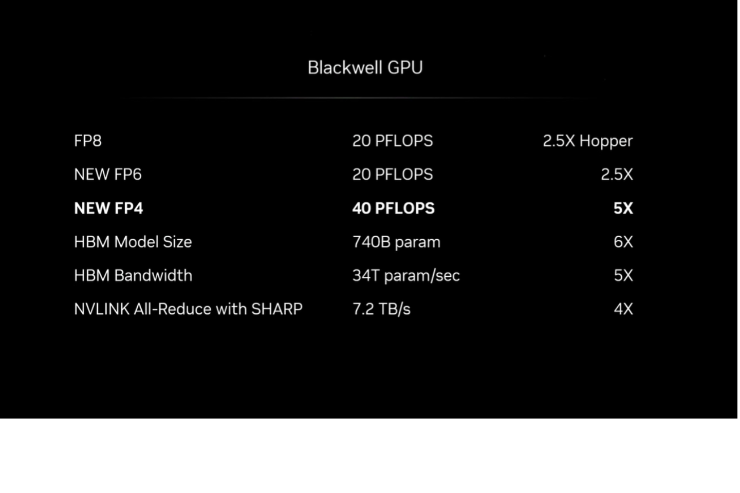
Compute Performance
- Optimized tensor cores support operations down to FP4 precision, enabling up to 10 PetaFLOPS of FP8 performance and 20 PFLOPS of FP4 performance for inference tasks, demonstrating significant progress in AI and machine learning capabilities.
NVLink Interconnect
- Utilizes the NV-High Bandwidth Interface (NV-HBI), offering 10TB/second of bandwidth for inter-die communication. This feature ensures the two dies operate seamlessly as one unified CUDA GPU, eliminating potential performance bottlenecks.
Efficiency and Performance
- Despite adhering to a 4nm-class TSMC 4NP manufacturing process, Blackwell achieves a 4x increase in training performance and a 30x improvement in inference performance, all while realizing 25x greater energy efficiency compared to earlier generations.
DGX B200 specifications
| Specification | Details |
|---|---|
| GPU | 8x NVIDIA B200 Tensor Core GPUs |
| GPU Memory | 1,440GB total GPU memory |
| Performance | 72 petaFLOPS training and 144 petaFLOPS inference |
| Power Consumption | ~14.3kW max |
| CPU | 2 Intel® Xeon® Platinum 8570 Processors (112 Cores total, 2.1 GHz Base, 4 GHz Max Boost) |
| System Memory | Up to 4TB |
| Networking | 4x OSFP ports serving 8x single-port NVIDIA ConnectX-7 VPI (Up to 400Gb/s InfiniBand/Ethernet) |
| 2x dual-port QSFP112 NVIDIA BlueField-3 DPU (Up to 400Gb/s InfiniBand/Ethernet) | |
| Management Network | 10Gb/s onboard NIC with RJ45, 100Gb/s dual-port ethernet NIC, Host BMC with RJ45 |
| Storage | OS: 2x 1.9TB NVMe M.2, Internal: 8x 3.84TB NVMe U.2 |
| Software | NVIDIA AI Enterprise, NVIDIA Base Command™, DGX OS / Ubuntu |
| Rack Units (RU) | 10 RU |
| System Dimensions | Height: 17.5in (444mm), Width: 19.0in (482.2mm), Length: 35.3in (897.1mm) |
| Operating Temperature | 5–30°C (41–86°F) |
| Enterprise Support | Three-year Enterprise Business-Standard Support, 24/7 portal access, Live agent support during business hours |